Deciphering the ASIC Design Flow: A Comprehensive Exploration
Application-Specific Integrated Circuits (ASICs) quietly orchestrate the intricate symphony of modern electronics, tailored to deliver precise, efficient performance. From the smartphone in your palm to the data center processing your online activities, ASICs are the unassuming heroes. Yet, birthing these electronic maestros requires navigating a labyrinthine process known as the ASIC design flow.

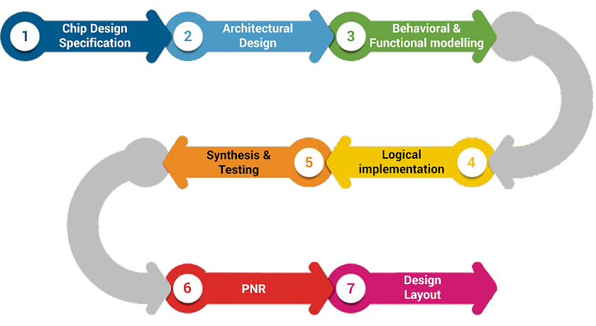
The journey commences with specifications, where engineers collaboratively craft the chip’s mission, defining its purpose, performance benchmarks, power needs, and physical boundaries. These specifications serve as the guiding constellation for architectural design, sketching the chip’s blueprint, determining its major functional components, and plotting the web of interconnections. The design then plunges into the Register Transfer Level (RTL) realm. Here, engineers wield specialized Hardware Description Languages (HDLs) like Verilog or VHDL, composing code that spells out the chip’s logic gate-level functionality. Stringent verification ensues, scrutinizing the RTL design to align with the specified requirements while eradicating any lurking logical gremlins.
Once the logical design is vetted, synthesis emerges, alchemizing the high-level code into a netlist of logical gates. Synthesis tools deftly optimize this gate-level design, considering factors such as real estate, speed, and power efficiency. The physical design phase unveils its canvas, featuring floor planning where logical blocks and their intricate dance are choreographed. Then, the chip’s placement takes center stage, followed by the artful weaving of interconnections between these blocks — a meticulous ballet that births the physical embodiment of the ASIC. Enter Design for Test (DFT), a critical performer ensuring the chip’s testability during production. Timing analysis and optimization fine-tune the performance, guaranteeing that signals waltz harmoniously within the chip, hitting their cues to meet specified clock frequencies.
Sign-off procedures perform the last bow, confirming the design’s harmony with all requirements before the ASIC sets off for its manufacturing voyage, often dubbed “tapeout.” The manufacturing tableau unfurls, etching the ASIC design into a silicon wafer through advanced lithographic techniques.
A rigorous testing overture ensues to unmask any manufacturing blemishes. Post-testing, the chips find refuge in their protective casings, where they are bestowed with electrical connections. Then, they take their rightful place, integrating into the final product. Post-silicon validation — the grand finale — presents comprehensive testing under real-world conditions, with any discoveries choreographing future design refinements.
The ASIC design flow is a labyrinthine odyssey, a symphony of expertise in electronics, digital logic, and semiconductor wizardry. In a world where tailored, efficient solutions reign supreme, ASICs remain steadfastly in the spotlight, composing the future of electronics.
Comments
Post a Comment